In today’s rapidly evolving electronics industry, high speed stamping has emerged as a cornerstone technology, revolutionizing how we manufacture a wide range of electronic devices. From smartphones to complex circuit boards, this process enables us to produce high-precision components efficiently, meeting the growing demands for smaller, faster, and more reliable electronics. Let’s delve deeper into the various aspects of how high speed stamping plays a crucial role in the electronics sector.
1. The Core Advantages of High Speed Stamping in Electronics Manufacturing
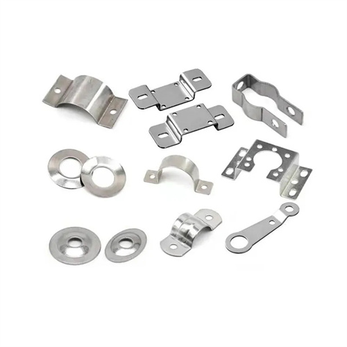
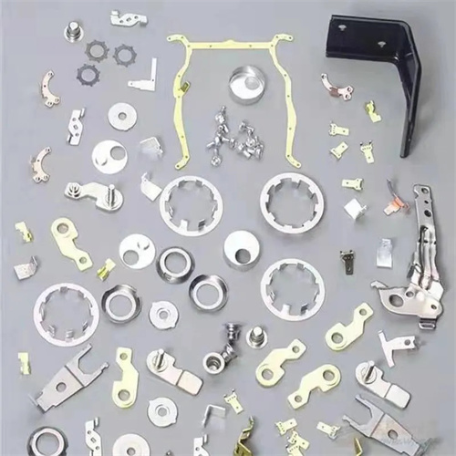
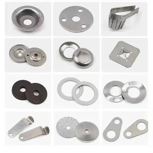
High speed stamping offers us several key advantages that are indispensable in electronics production. First and foremost, its ability to achieve high precision is remarkable. With advanced die designs and high-speed presses, we can create components with intricate geometries and tight tolerances. For instance, in the production of connectors, the fine pins and sockets need to be crafted with utmost accuracy to ensure proper electrical connections. High speed stamping allows us to produce these parts with micrometer-level precision, ensuring seamless integration into electronic devices. Additionally, the repeatability of this process guarantees that each component meets the same high standards, enhancing the overall quality and reliability of the final products.
2. Boosting Production Efficiency with High Speed Stamping
One of the most significant benefits of high speed stamping for us in the electronics industry is the substantial increase in production efficiency. Unlike traditional manufacturing methods, high speed stamping can produce a large number of components in a short period. High-speed presses can operate at extremely fast cycles, sometimes producing hundreds of parts per minute. This high output rate is crucial for meeting the mass production requirements of the electronics market, where consumer demand for products like smartphones and tablets is constantly high. Moreover, the automated nature of high speed stamping reduces the need for manual intervention, minimizing errors and further enhancing productivity.
3. Cost – Effective Solutions Enabled by High Speed Stamping
Cost control is a major concern in electronics manufacturing, and high speed stamping provides us with effective cost – saving solutions. Although the initial investment in high speed stamping equipment and dies can be significant, the long – term benefits far outweigh the costs. Due to its high production speed and efficiency, the cost per unit of components produced through high speed stamping is relatively low. Additionally, the reduction in labor costs associated with automated production and the minimized material waste due to precise stamping contribute to overall cost savings. This makes high speed stamping an economically viable option for producing a wide variety of electronic components, from small fasteners to large heat sinks.
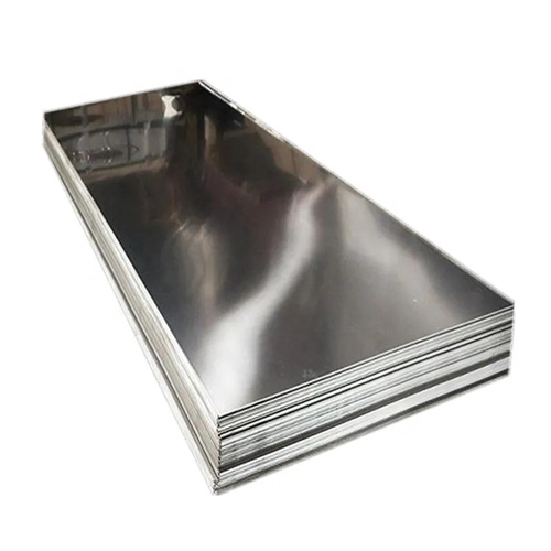
4. Material Selection and Adaptability in High Speed Stamping for Electronics
The success of high speed stamping in electronics also lies in its adaptability to different materials. We have a wide range of materials at our disposal, including various metals such as copper, aluminum, and stainless steel, as well as some specialty alloys. Each material has unique properties that are suitable for different electronic applications. For example, copper is often used for components that require high electrical conductivity, while aluminum is preferred for parts where lightweight and good heat dissipation are necessary. High speed stamping can handle these diverse materials effectively, with proper die design and process optimization. This allows us to choose the most appropriate material for each component, ensuring optimal performance of the electronic devices.
5. Quality Assurance in Electronics through High Speed Stamping
Maintaining high quality is non – negotiable in the electronics industry, and high speed stamping has built – in mechanisms for quality assurance. Advanced monitoring systems are integrated into high speed stamping equipment to detect any deviations in the stamping process in real – time. For example, sensors can measure the thickness of the stamped parts, the force applied during stamping, and the temperature of the dies. Any anomalies are immediately flagged, allowing us to take corrective actions promptly. Additionally, the use of high – quality dies and regular maintenance of the stamping equipment further ensures consistent quality. This strict quality control throughout the high speed stamping process guarantees that the electronic components we produce meet the stringent industry standards.